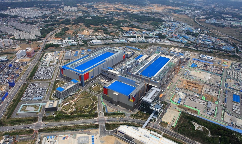
US President Joe Biden is visiting South Korea starting today, and his first stop will be Samsung's semiconductor factory in Pyongyang. Samsung Electronics Vice Chairman Lee Jae-yong will reportedly tour the factory, which is the largest of its kind in the world.
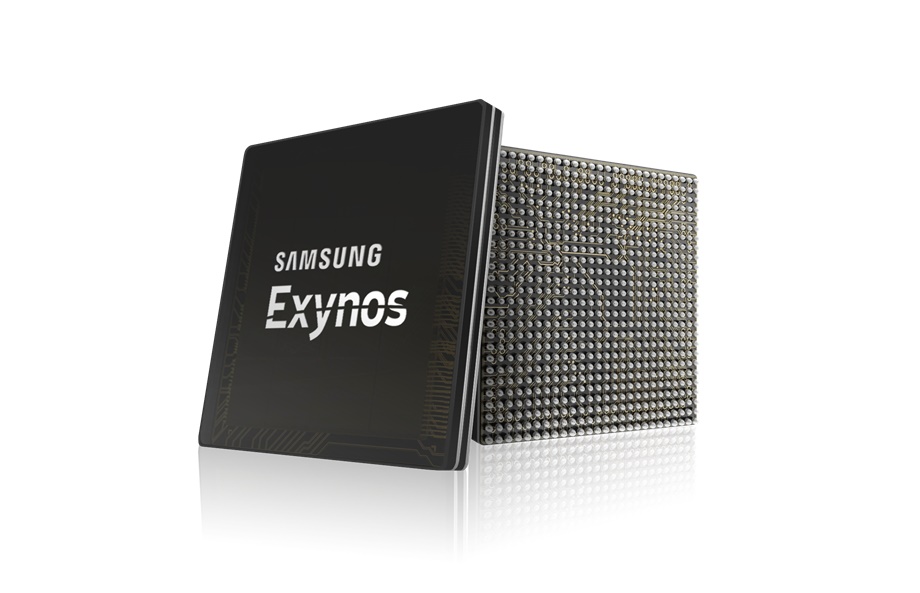
Lee is expected to show Biden the upcoming 3nm GAA chips, manufactured by the Samsung Foundry division. GAA (Gate All Around) technology is used by the company for the first time in its history. It has previously said it will begin mass production of 3nm GAA chips in the next few months. These chips are said to offer 30% higher performance than 5nm chips and up to 50% lower power consumption. It's also worth noting that there is a 2nm manufacturing process in early development that should start sometime in 2025.
You could be interested in

In the past few years, Samsung's chip manufacturing technology has lagged behind its arch-rival TSMC, both in terms of yield and energy efficiency. The Korean giant has lost large clients such as Apple a Qualcomm. With 3nm GAA chips, it could finally catch up or even overtake TSMC's 3nm chips.
