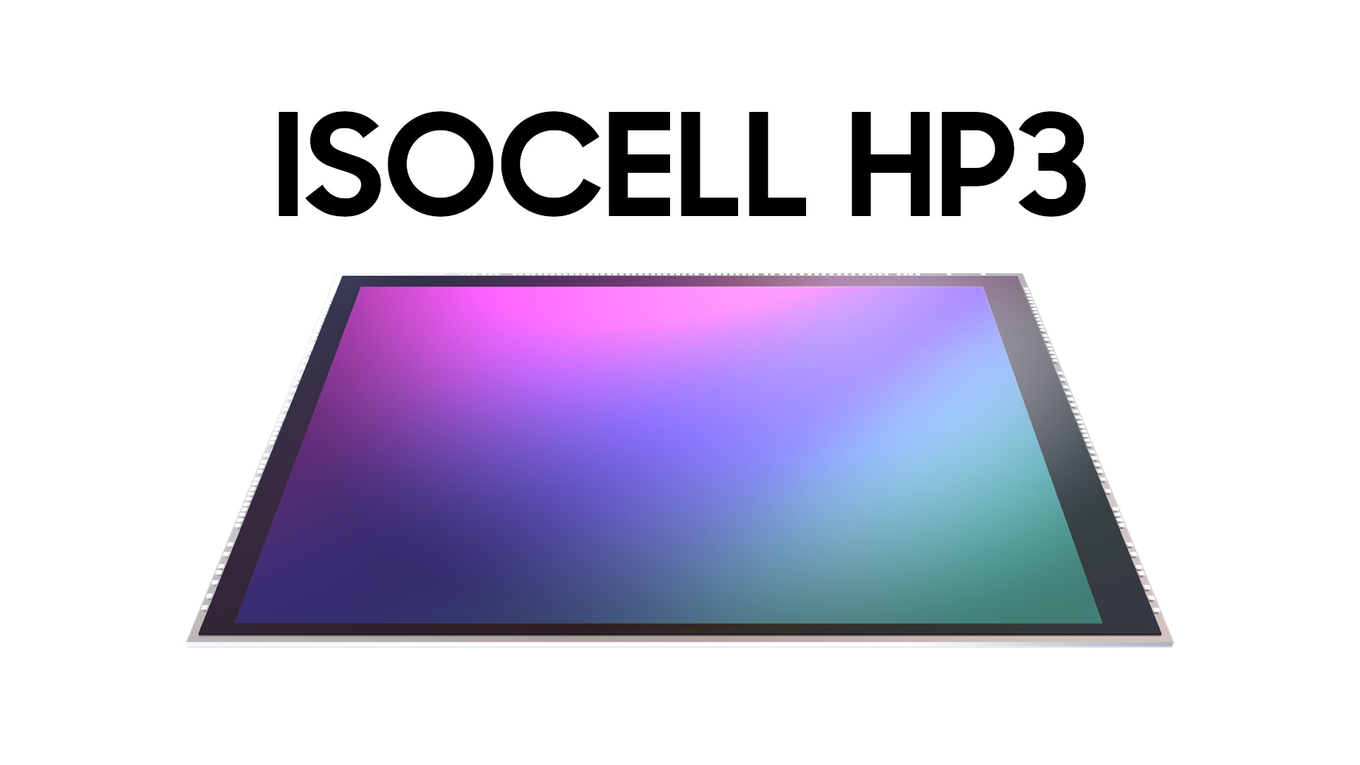
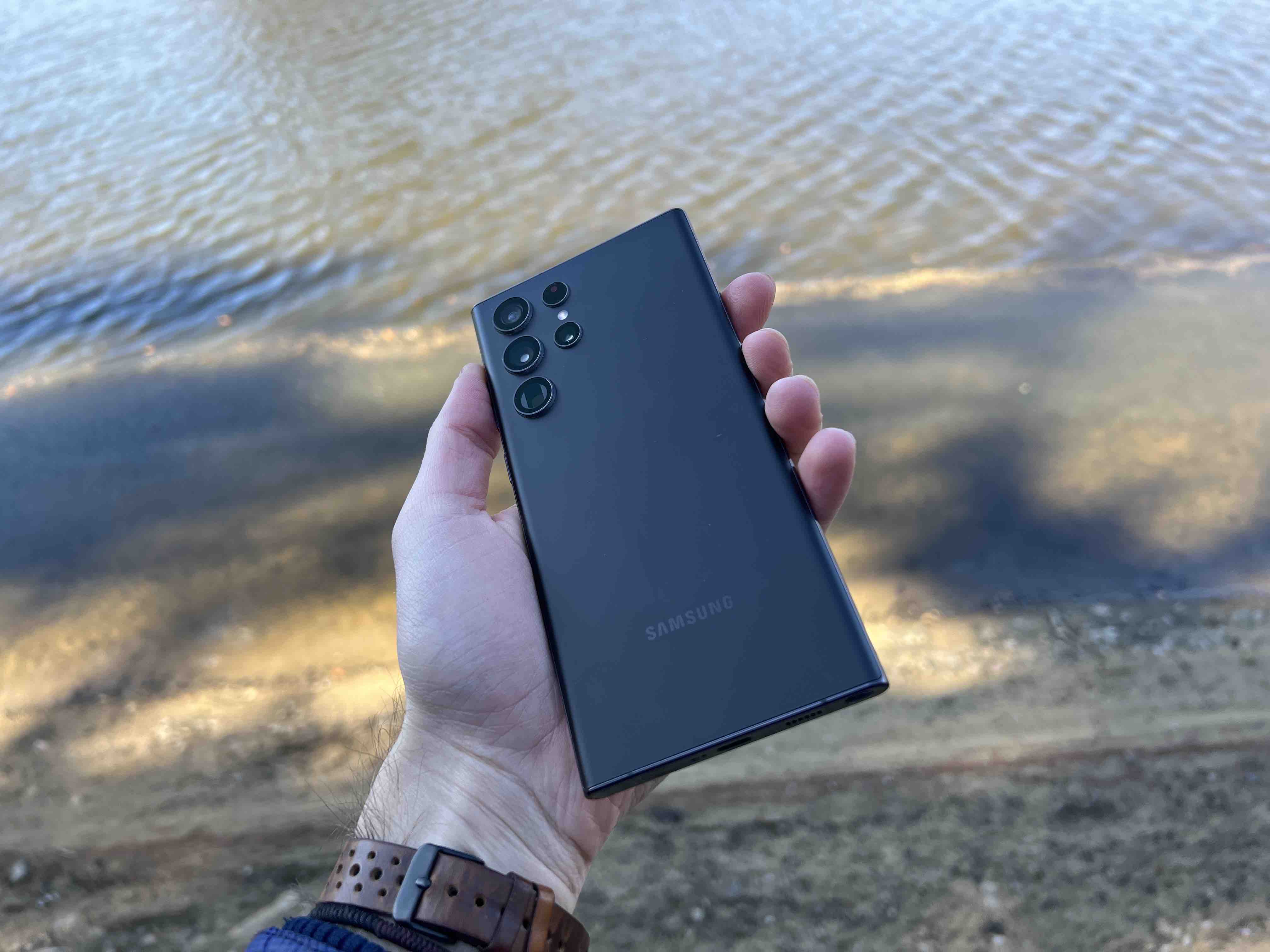
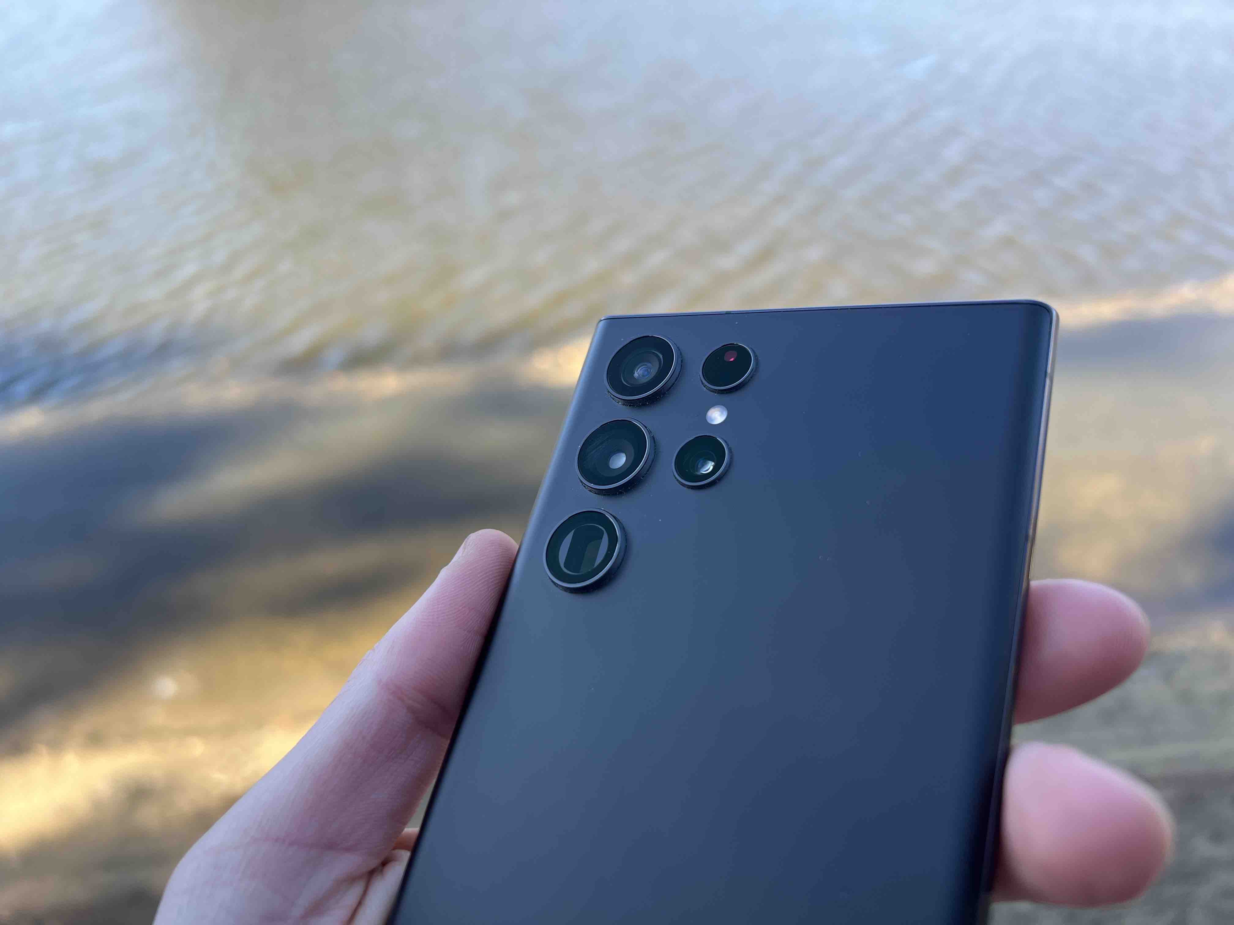
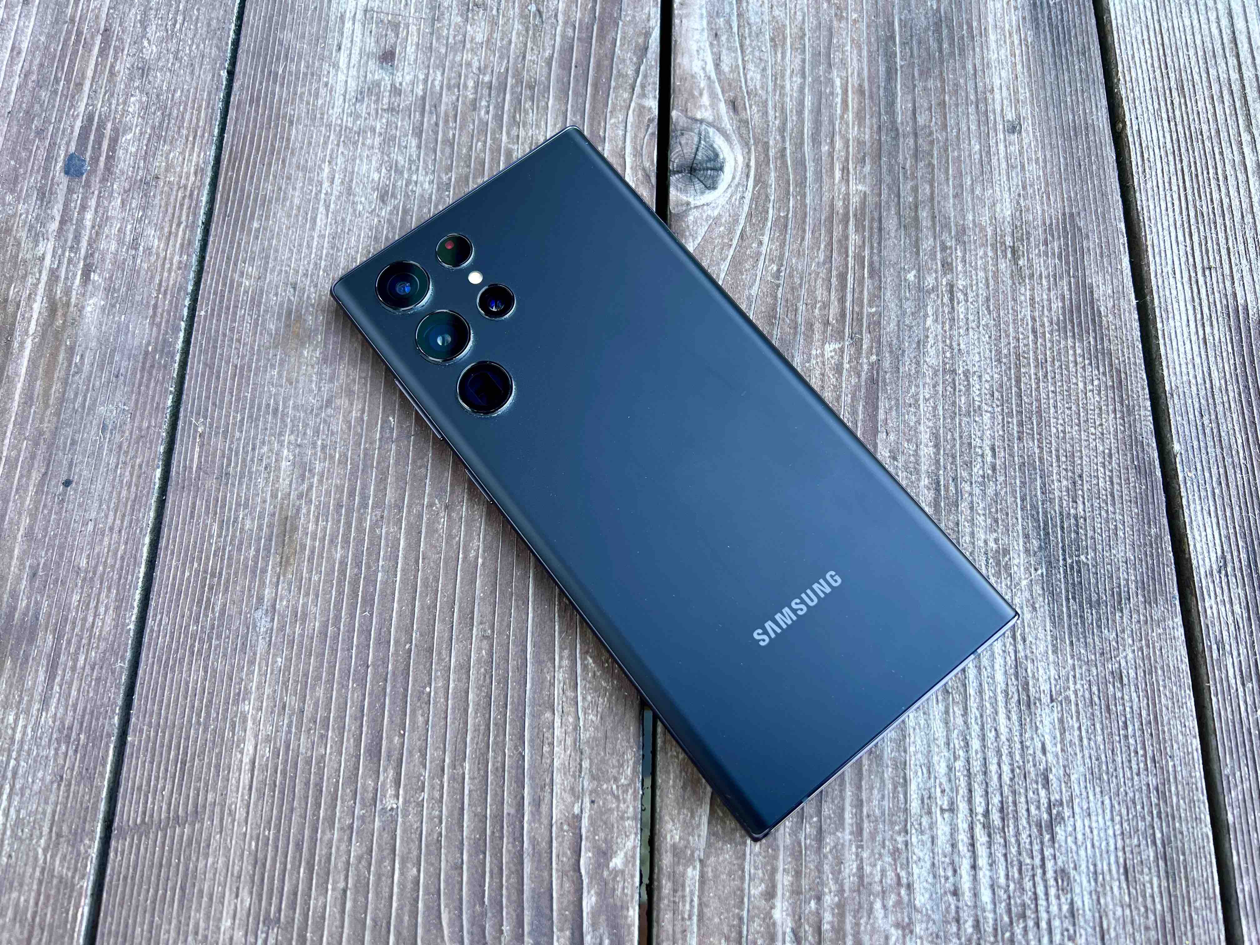
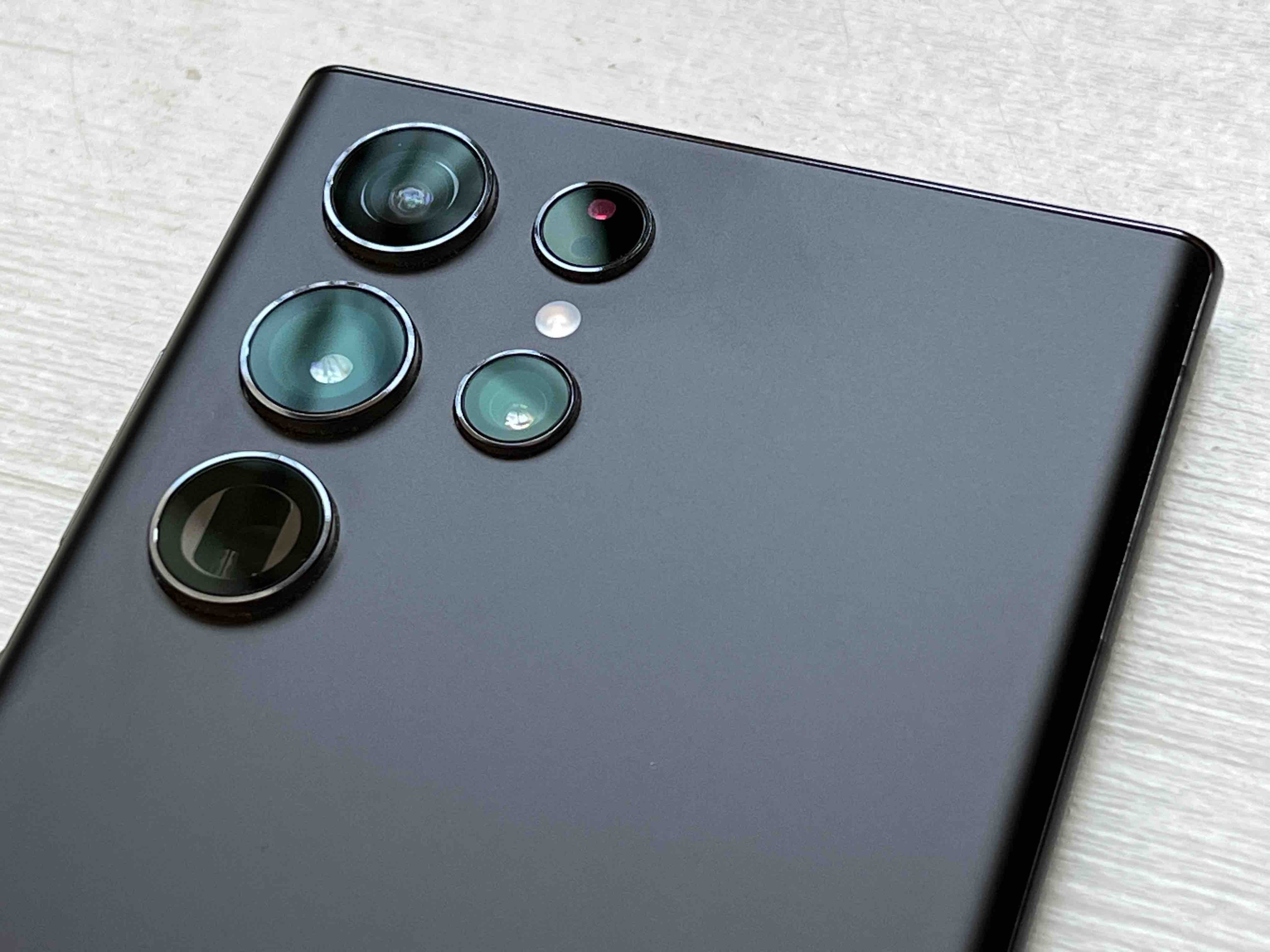
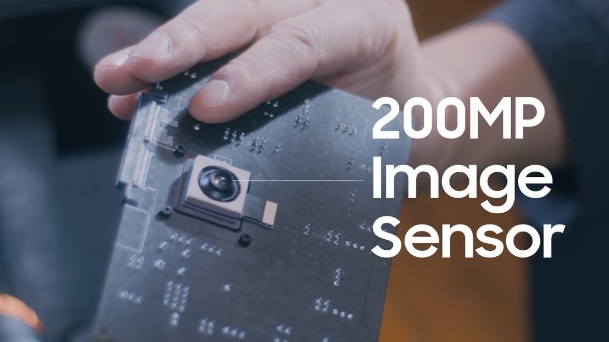
Samsung introduced a new 200MPx photo sensor a few weeks ago ISOCELL HP3. This is the sensor with the smallest pixel size ever. Now, the Korean tech giant has talked about its development through developers from the System LSI division and the Semiconductor R&D Center.
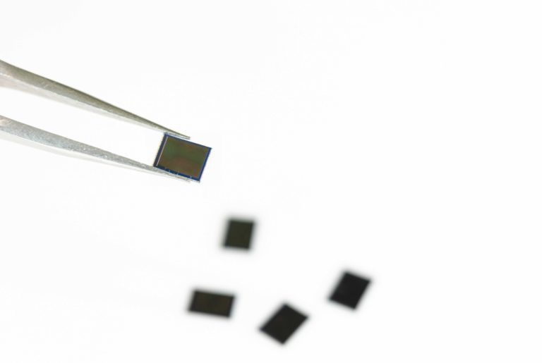
An image sensor (or photosensor) is a system semiconductor that converts the light that enters the device through the camera lens into digital signals. Image sensors are built into all electronic products that have a camera, such as digital cameras, laptops, cars and, of course, smartphones. The ISOCELL HP3, introduced by Samsung in June, is a photosensor that contains 200 million 0,56 micron pixels (the industry's smallest pixel size) in a 1/1,4" optical format.
"With smaller individual pixel sizes, the physical size of the sensor and module can be reduced, which also allows the size and width of the lens to be reduced," explains developer Myoungoh Ki from Samsung's System LSI division. "This can eliminate elements that detract from the device's design, such as a protruding camera, as well as reduce power consumption," added.
While smaller pixels allow the device to be slimmer, the key is to maintain image quality. ISOCELL HP3, developed using state-of-the-art technologies, with 12% smaller pixel size than Samsung's first 200MPx photosensor ISOCELL HP1, can reduce the surface area of the camera in a mobile device by up to 20%. Despite the smaller pixel size, ISOCELL HP3 has been developed using technology that maximizes their Full Well Capacity (FWC) and minimizes loss of sensitivity. Smaller pixel size is ideal for creating smaller, slimmer devices, but can result in less light entering the device or interference between neighboring pixels. However, even with this, Samsung was able to cope, and according to Ki, it is thanks to the proprietary technological capabilities of the Korean giant.
Samsung has managed to create physical walls between pixels that are thinner and deeper using Full Depth deep trench isolation (DTI) technology, which guarantees high performance even at a size of 0,56 microns. DTI creates an isolated component between pixels that acts as an insulating wall to prevent light loss and improve optical performance. Developer Sungsoo Choi of Samsung's Semiconductor R&D Center compares the technology to building a thin barrier between different rooms in a building. "In layman's terms, it's the same as trying to create a thinner wall between your room and the room next door without affecting the level of soundproofing," he explained.
You could be interested in
Super Quad Phase Detection (QPD) technology allows all 200 million pixels to focus by increasing the intensity of the autofocus pixels to 100%. QPD offers a faster and more accurate autofocus function by using a single lens over four pixels, allowing the measurement of all phase differences of the left, right, top and bottom of the subject being photographed. Not only is the autofocus more accurate at night, but the high resolution is maintained even when zoomed in. To deal with the problem of poor image quality in low-light environments, Samsung used innovative pixel technology. "We used an improved version of our proprietary Tetra2pixel technology, which combines four or sixteen adjacent pixels to act as one large pixel in low-light environments," Choi said. The improved pixel technology makes it possible to shoot videos in 8K resolution at 30 fps and in 4K at 120 fps without losing the field of view.
Ki and Choi also said that they encountered a number of technical obstacles in the development of the new photosensor (especially in the implementation of DTI technology, which was used by Samsung for the first time), but that they were overcome thanks to the cooperation of various teams. Despite the demanding development, the Korean giant introduced the new sensor less than a year after announcing its first 200MPx sensor. What smartphone it will debut in is still unclear at this point.
